
AdPac-in
Advanced Packaging with Computational Intelligence (AdPac-In) is a multidisciplinary research group at the School of Mechanical Engineering, Universiti Sains Malaysia, advancing the mechanics, reliability, and computational design of next-generation semiconductor packaging technologies. The group integrates fundamental mechanics, , computational fluid dynamics, finite-element and multiphysics simulation, interfacial engineering, data-driven modelling, and computational intelligence to address increasingly complex reliability challenges associated with heterogeneous integration, three-dimensional packaging, fine-pitch interconnects, and highly miniaturised electronic systems.
AdPac-In focuses on understanding how packaging architecture, material behaviour, interfacial interactions, and manufacturing-induced thermal loading collectively govern deformation, stress evolution, damage accumulation, and long-term package reliability. Rather than treating simulation solely as a post-design verification tool, the group develops simulation-driven and intelligence-assisted design approaches that relate geometric and physical design parameters to reliability performance. This research direction supports high-performance and high-reliability semiconductor packaging while bridging fundamental mechanics with scalable engineering solutions for future electronic systems.
Group members
|
Professor Ir. Dr. Mohd. Zulkifly Bin Abdullah (Chairman)
Area of Expertise: Electronic Packaging in 3D Packaging and TSV, Advanced Electronic Cooling for High Heat Flux, Porous Medium Burner for Domestic Applications |

|
Associate Professor Ts. Dr. Mohd Sharizal Abdul Aziz (Head) |

|
Professor Ir. Ts. Dr. Mohammad Aizat bin Abas (Member) |

|
Associate Professor Dr. Abdullah Aziz bin Saad (Member) |

|
Ir. Dr. Mohd Syakirin bin Rusdi (Member) |

|
Mrs. Zuraihana binti Bachok (Member) |

|
Mr. Roslan bin Kamarudin (Member) |

Research capabilities
i) Advanced Packaging and 3D Integration
AdPac-In investigates the mechanical and thermo-mechanical behaviour of advanced semiconductor packages in which continued miniaturisation, heterogeneous integration, and increasing interconnect density create reliability challenges that cannot be adequately understood through conventional package-level design rules alone. Particular emphasis is placed on three-dimensional integration, fine-pitch interconnect structures, direct Cu-Cu bonding, hybrid-bonding architectures, stacked semiconductor dies, and related emerging packaging configurations.
At progressively smaller length scales, reliability becomes increasingly dependent on the interaction among interconnect geometry, silicon stiffness, interfacial constraint, thermal-expansion mismatch, and spatial support topology. The package is therefore examined as an interconnected mechanical system rather than as isolated materials or components. This approach enables assessment of how local interconnect behaviour propagates towards die-scale warpage, stress redistribution, interfacial loading, and package-level reliability.
One active research stream examines direct Cu-Cu bonded stacked-die architectures in which interconnect height, diameter, pitch, population, and spatial configuration are systematically varied to determine their influence on thermally induced deformation and stress. The objective is not merely to identify a single favourable geometry, but to establish mechanistic design principles explaining how interconnect architecture controls structural compliance, silicon support, local copper accommodation, and global package response.
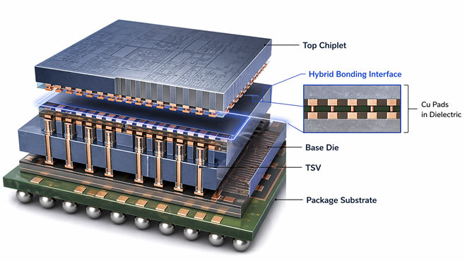
Figure: Hybrid Bonding Advanced Packaging
ii) Thermo-Mechanical and Multiphysics Modelling
Computational modelling forms a central component of AdPac-In research. Finite-element and multiphysics approaches are employed to resolve the coupled physical behaviour of advanced semiconductor packages under manufacturing, environmental, and operational loading conditions. These models enable temperature evolution, thermal deformation, interfacial constraint, stress redistribution, and material inelasticity to be evaluated at spatial and temporal scales that are difficult to access experimentally.
For stacked-die and direct-bonding applications, sequential thermal-structural modelling can reproduce thermal-cycling conditions and transfer transient temperature fields into detailed structural analyses. Depending on the problem, the framework may incorporate anisotropic silicon behaviour, temperature-dependent copper properties, time-dependent deformation, interfacial thermal conductance, and geometrically resolved micro-interconnect structures. Experimental temperature and deformation measurements can subsequently be used to establish confidence in the numerical framework before extensive parametric investigations are undertaken.
This modelling philosophy is particularly important because local and global reliability responses may not evolve identically. A design that reduces package warpage may simultaneously intensify loading within a specific interconnect region, while a configuration that lowers local copper stress may impose additional constraint on the silicon. AdPac-In therefore evaluates multiple physical responses when assessing advanced packaging reliability.
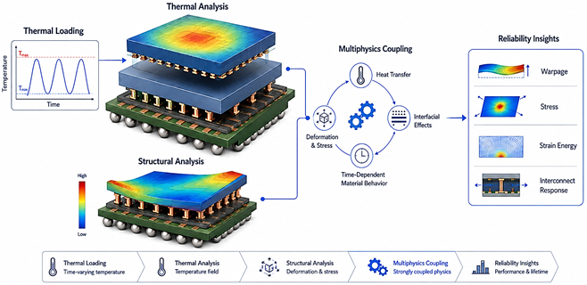
Figure: Multiphysics coupling workflow
iii) Interconnect Architecture and Reliability Mechanics
A major research theme within AdPac-In concerns the relationship between interconnect architecture and structural reliability. As interconnect dimensions approach increasingly fine scales, geometric parameters cannot be considered independently because their mechanical consequences are mediated by the collective stiffness and spatial continuity of the entire interconnect network.
Studies of direct Cu-Cu bonded structures therefore investigate how interconnect height, diameter, pitch, and spatial arrangement modify package compliance and the transfer of thermo-mechanical loads between adjoining silicon dies. Taller or more compliant interconnect structures may enable greater local deformation accommodation, whereas variations in diameter and pitch alter both local load-bearing behaviour and the effective stiffness of the bonded region. Importantly, the total number of interconnects alone does not necessarily determine mechanical performance; their spatial distribution can be equally or more influential than their absolute population.
This principle is especially relevant to non-uniform interconnect configurations. Spatial discontinuities, unsupported silicon regions, peripheral reinforcement, and local changes in structural restraint can substantially alter the deformation field even when overall interconnect populations remain similar. Topology-aware analysis therefore provides a pathway towards layouts that balance warpage suppression, silicon protection, interconnect stress control, and cyclic reliability. The broader objective is to move advanced packaging design from empirical geometric selection towards mechanics-informed architectural design, where spatial interconnect topology becomes an explicitly engineered reliability variable.
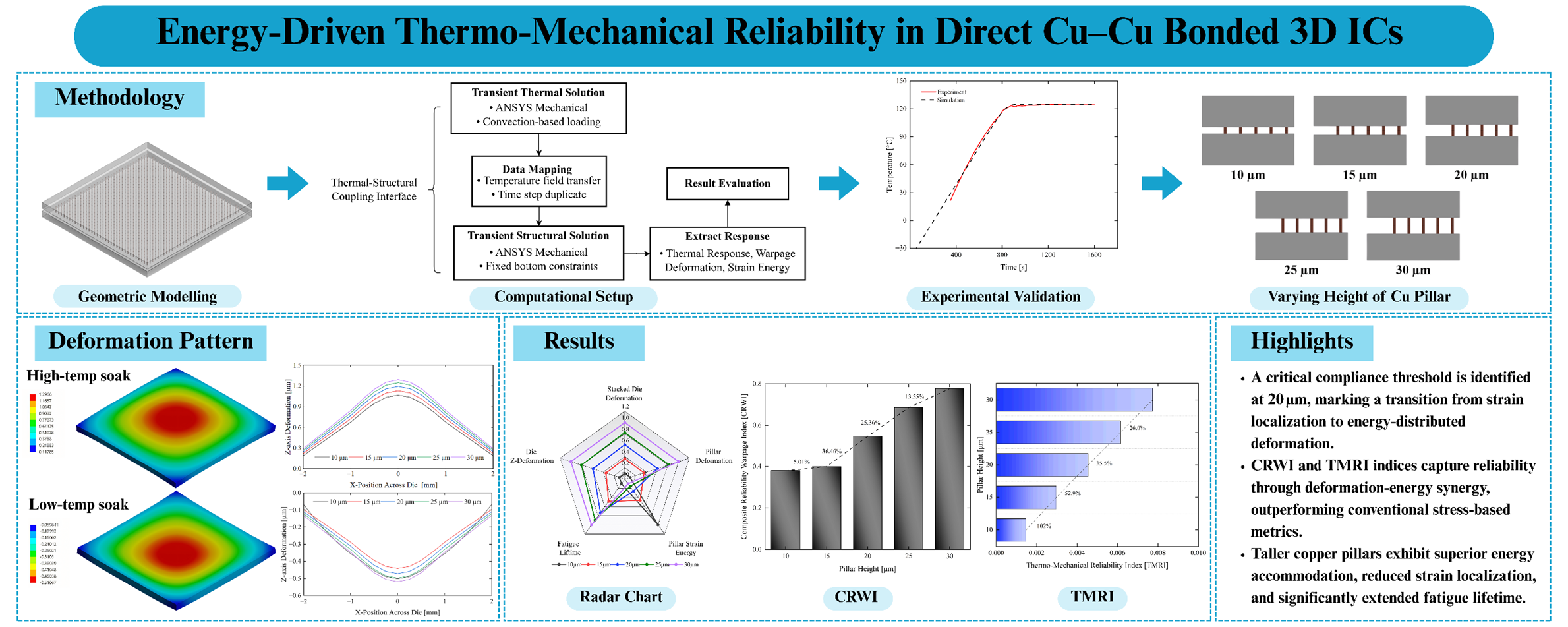
Figure: Geometric of interconnect on the structural reliability
iv) Computational Intelligence and Data-Driven Reliability
The computational-intelligence component distinguishes AdPac-In from a purely numerical simulation research group. High-fidelity finite-element simulations generate multidimensional information, but the engineering value of those simulations depends on converting numerical responses into interpretable design knowledge. AdPac-In therefore seeks to integrate physics-based modelling with statistical learning, optimisation, probabilistic analysis, and artificial-intelligence-assisted methods.
Within advanced packaging reliability studies, computational intelligence can be used to identify influential design parameters, reveal nonlinear interactions among geometric descriptors, construct surrogate models, rank competing architectures across multiple reliability objectives, and generate predictive relationships that complement conventional finite-element analysis. Multi-response decision frameworks are particularly useful when improvements in one reliability metric occur at the expense of another, allowing design alternatives to be assessed according to their overall thermo-mechanical balance rather than a single isolated response.
More advanced formulations can relate numerical reliability outcomes to physically interpretable geometric descriptors. Descriptors representing peripheral support, unsupported silicon area, interconnect-density distribution, or spatial discontinuity can be evaluated probabilistically to identify architectural characteristics that consistently govern mechanical performance. In this framework, computational intelligence does not replace physics-based simulation; it acts as an interpretive layer that converts simulation databases into generalisable engineering knowledge.
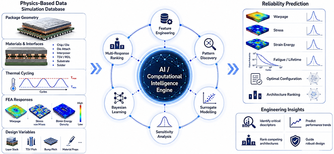
Figure: Pipeline of computational intelligence
v) Thermal-Cycling Reliability and Experimental Validation
Numerical reliability predictions gain substantial value when their governing assumptions are assessed against physical measurements. AdPac-In therefore supports the integration of computational modelling with experimentally informed validation strategies wherever appropriate. For thermo-mechanical packaging studies, controlled thermal cycling can reproduce repeated temperature excursions associated with qualification or service environments, while temperature measurements provide direct assessment of transient thermal predictions. Complementary deformation measurements can then evaluate whether the structural model correctly captures the thermo-mechanical response of the assembly.
This combined methodology establishes a closed research loop in which experiments provide physical grounding for numerical models, simulations provide access to internal fields that are difficult to measure directly, and subsequent computational analysis enables substantially larger design spaces to be investigated than would be practical through experiments alone.
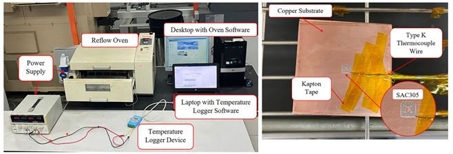
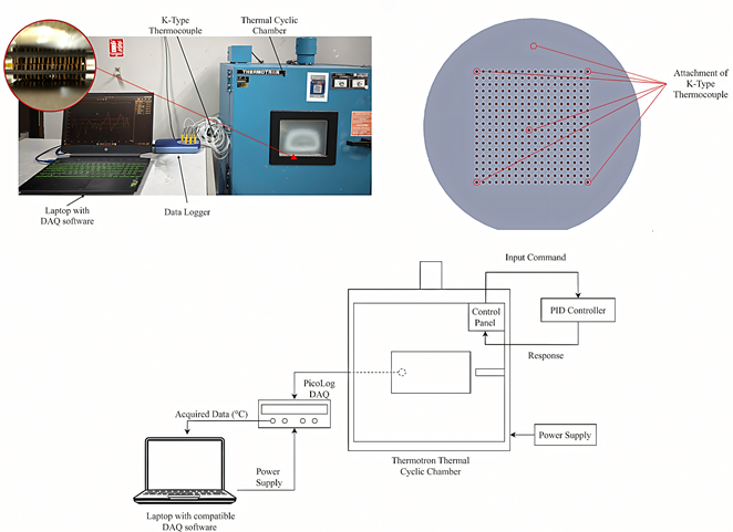
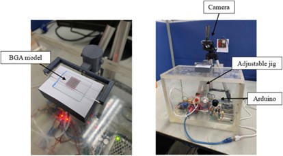
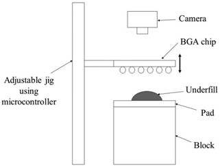
Figure: Experimental testing workflow
iv) Underfill, Encapsulation and Packaging Process Reliability
AdPac-In investigates underfill and encapsulation processes in flip-chip, BGA, multi-stack and heterogeneous electronic packages, with emphasis on flow behaviour, void formation and process-induced reliability. Computational fluid dynamics and multiphysics modelling are used to examine the effects of package geometry, interconnect configuration, material properties and processing conditions on encapsulant flow and defect formation. These physics-based approaches are increasingly integrated with machine learning and data-driven analysis to support defect prediction, process optimisation and improved packaging reliability.
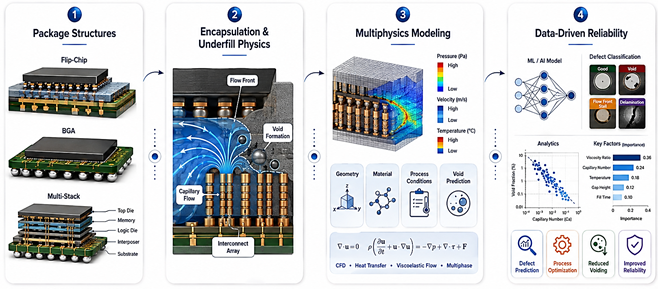
Figure: Underfill encapsulation
Research Partnership and Industrial Collaboration
AdPac-In places emphasis on connecting computational and fundamental research with the needs of the semiconductor industry. Existing activities include collaborative analysis with the Synchrotron Light Research Institute in Thailand for materials characterisation, industrial engagement with Intel and SanDisk, and the USM-Intel Advanced Packaging Research Collaboration. These partnerships provide an important interface between fundamental research questions and technologically relevant packaging challenges.
The group's research model is therefore centred on industry-relevant fundamental mechanics: practical packaging challenges motivate research questions, high-fidelity computation is used to identify the governing physical mechanisms, and computational intelligence converts those findings into actionable design knowledge. This interaction supports both scientific development and the translation of advanced packaging research towards future manufacturing applications.
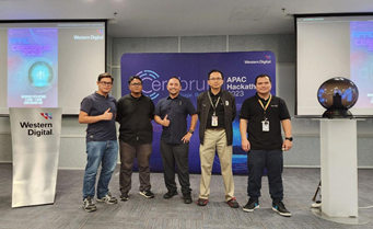
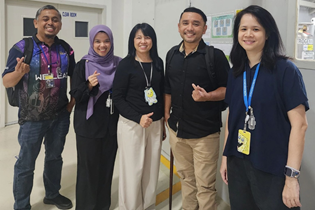
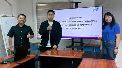
Figure: Collaboration with Industry Partners
Research Impact and Contributions
AdPac-In seeks to contribute to advanced semiconductor packaging at three interconnected levels. At the fundamental level, the group investigates the mechanics governing deformation, stress transfer, interfacial behaviour, and damage accumulation in increasingly heterogeneous and miniaturised electronic structures. At the engineering level, simulation and optimisation are used to translate these mechanisms into improved interconnect dimensions, layouts, and package architectures. At the strategic level, the group contributes towards strengthening national capabilities in semiconductor packaging research by developing modelling knowledge, research talent, and industry-linked expertise within Malaysia.
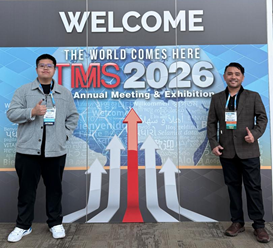
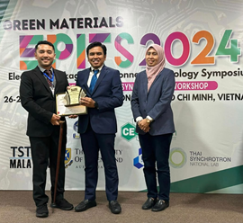
Figure: TMS 2026 Conference and EPITS 2024 Symposium
Future Research Direction
Future AdPac-In research will progressively move beyond isolated geometric optimisation towards integrated physics-intelligence frameworks for advanced packaging design. Emerging directions include ultra-fine-pitch direct and hybrid bonding, chiplet and heterogeneous integration, interface-aware reliability modelling, manufacturing-process-structure relationships, multi-scale thermo-mechanical analysis, probabilistic reliability prediction, surrogate modelling, explainable machine learning, and AI-assisted optimisation of interconnect architectures.
A particularly important trajectory is the transition from conventional parameter-based analysis towards architecture-aware reliability engineering. Rather than asking only what interconnect diameter, height, or pitch should be selected, future research can investigate how complete interconnect networks should be spatially organised to produce prescribed mechanical responses. Combined with physically interpretable data-driven models, this creates the possibility of inverse packaging design in which required reliability targets guide the generation of suitable interconnect architectures.
In the longer term, integrating validated multiphysics simulation, experimental characterisation, semiconductor manufacturing data, and computational intelligence could support digital design frameworks capable of predicting packaging behaviour before extensive fabrication and qualification. Such a framework would strengthen AdPac-In as a platform for mechanics-informed intelligent design of next-generation semiconductor packages while supporting Malaysia's broader semiconductor manufacturing ecosystem.
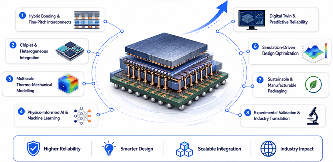
Figure: Future research roadmap and prospective advancement
Selected publications
-
Wong Y.J., Abdul Aziz M.S., Khor C.Y., Ishaik M.H.H., Yeoh K.H., Ang C.S., Energy-driven thermo-mechanical reliability in direct Cu–Cu bonded 3D ICs, International Journal of Mechanical Sciences, 2026, 309:111024.
2. Wong Y.J., Abdul Aziz M.S., Khor C.Y., Yeoh K.H., Ang C.S., Tan T.H.J., Thermomechanical correlation of interfacial shear and warpage in Cu–Cu bonded 3D stacked die packages thermal cycling, TMS 2026 155th Annual Meeting & Exhibition Supplemental Proceedings, The Minerals, Metals & Materials Series, 2026, 928–941.
3. Wong Y.J., Abdul Aziz M.S., Khor C.Y., Yeoh K.H., Ang C.S., Tan T.H.J., Zone-based thermo-mechanical gradient mapping in Cu–Cu bonded 3D stacked die packages for reliability analysis, TMS 2026 155th Annual Meeting & Exhibition Supplemental Proceedings, The Minerals, Metals & Materials Series, 2026, 942–956.
4. Ramalingam K., Abdullah M.Z., Abas M.A., Yu K.H., Kamarudin R., Rahman M.R.A., Wong S.F., Lam P.K., Cheah B.E., Semiconductor wafer warpage in electronics packaging: A hybrid investigation with ML and experimental insights, The International Journal of Advanced Manufacturing Technology, 2026, 142:1765–1781.
5. Liu J., Saad A.A., Zheng Y., Ji H., Bachok Z., Anand model and finite element analysis of Sn-0.3Ag-0.7Cu-3Bi lead-free solder joints in BGA packages, Materials, 2026, 19(3):636.
6. Abas A., Muhamed Mukhtar M.A.F., Numerical simulation and multi objectives optimization of fillet height in reinforced SAC305 solder joints for ultrafine capacitor assemblies, Soldering & Surface Mount Technology, 2026, 38(1):61–76.
7. Lee J.R., Abdul Aziz M.S., Khor C.Y., Ishaik M.H.H., Simanjuntak J.P., Wong Y.J., Thermal-mechanical analysis of copper pillar pitch size during reflow soldering assembly process, Microelectronics Reliability, 2025, 172:115827.
8. Azman M.A., Abdullah M.Z., Loh W.K., Ooi C.K., Flow characterization of capillary underfill in multi-chip heterogenous integration using computational fluid dynamics, Journal of Electronic Packaging, 2025, 147(3).
9. Ling C., Azahari M.T., Abas M.A., Ng F.C., Correlation study on voiding in underfill of large quantity ball grid array chip using machine learning, Journal of Electronic Packaging, 2025, 147(1):011001.
10. Aman N.A.M.N., Abdullah M.Z., Loh W.K., Ooi C.K., Influence of die and lid shapes on void formation in solder thermal interface materials, Microelectronics Reliability, 2025, 173:115847.
11. Lee J.R., Abdul Aziz M.S., Khor C.Y., Ishaik M.H.H., Kamarudin R., Che Ani F., Impact of Cu pillar bump diameter and solder material on reflow soldering: A computational study with thermal fluid–structure interaction, Journal of Electronic Materials, 2024, 53(3):1201–1213.
12. Abas M.A., Muhamed Mukhtar M.A.F., Effects of different air gaps of underfill encapsulant on multi-stack printed circuit board, Microelectronics Reliability, 2024, 163:115533.
13. Ling C., Chew C.K., Abas M.A., Azahari M.T., Image segmentation on void regional formation in the flip-chip underfilling process by comparing YOLO and Mask RCNN, Soldering & Surface Mount Technology, 2024, 37(1):17–24.
14. Azman M.A., Abdullah M.Z., Loh W.K., Ooi C.K., Advancing packaging technology: Computational fluid dynamics modeling for capillary underfill encapsulant in multi-chip heterogenous packages, Soldering & Surface Mount Technology, 2024, 37(1).
15. Lee J.R., Abdul Aziz M.S., Mohd Salleh M.A.A., Khor C.Y., Ishaik M.H.H., Effects of diameter on copper pillar with solder cap interconnections during reflow soldering process, TMS 2023 152nd Annual Meeting & Exhibition Supplemental Proceedings, The Minerals, Metals & Materials Series, 2023, 909–920.
16. Ling C., Azahari M.T., Abas M.A., Ng F.C., Deep learning and analytical study of void regional formation in flip-chip underfilling process, Soldering & Surface Mount Technology, 2023, 36(1):60–68.
17. Lee J.R., Abdul Aziz M.S., Ishaik M.H.H., Khor C.Y., A review on numerical approach of reflow soldering process for copper pillar technology, The International Journal of Advanced Manufacturing Technology, 2022, 121(7–8):4325–4353.
18. Nashrudin M.N., Ng F.C., Abas M.A., Abdullah M.Z., Ali M.Y.T., Prediction of the void formation in no-flow underfill process using machine learning-based algorithm, Microelectronics Reliability, 2022, 135:114586.
19. Alim M.A., Abdullah M.Z., Abdul Aziz M.S., Kamarudin R., Gunnasegaran P., Recent advances on thermally conductive adhesive in electronic packaging: A review, Polymers, 2021, 13(19):3337.
20. Ng F.C., Zawawi M.H., Tung L.H., Abas M.A., Abdullah M.Z., Symmetrical unit-cell numerical approach for flip-chip underfill flow simulation, CFD Letters, 2020, 12(8):55–63.